
What Are The Different Types Of PCB Materials?
Know about the different types of PCB Materials
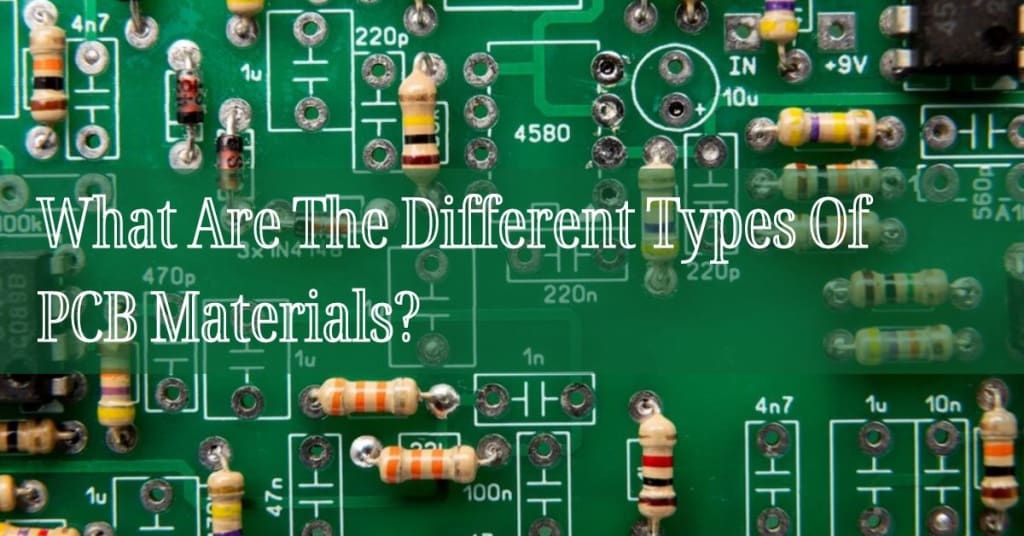
Printed Circuit Board (PCB) is one of the essential laminated boards that are useful to make the device and equipment operate. However, the PCB board is built with essential components like power supply, routing, electrical components, stacking, and network. The PCB design services layout the PCB board with precision between the laminated copper sheets on a non-substrate PCB. Thus, a regular PCB serves as a foundation for every electrical device. Hence, in this post, let us see the different types of PCB materials that various PCB manufacturers consider to layer the circuit board.
Selection process:
The foremost thing in PCB designing is the selection process. You have the select the materials or components for the board in respect of the physical, chemical, thermal, and electrical properties. So, here is a property list to choose the appropriate material for the PCB.
Thermal property: Choose the components that have higher temperature durability and constant peak distribution throughout designing the PCB circuit.
Mechanical property: You should choose the electrical component that has form factor management and enclosure including density and flexibility on the rigid boards.
Electrical property: Check on the components for the dielectric factors like resistances, signals, and impedance for the perfect balance of the circuit board.
Chemical property: Similarly, look for the moisture absorption, flammability, and humid factors for the lifespan of your components.
Silkscreen:
Another prime thing in choosing the PCB materials is the silkscreen. We all have a green board inside the device while repairing. The PCB board and silkscreen have been incorporated against the green board. The name is given due to the stenciling technique that is used in marking numbers, letters, and symbols on the board. The ports for component placing, location, and polarity are all designed with the help of silkscreen. The most common techniques used for designing the silkscreen are,
Liquid Photo Imaging (LPI): The most common technique that is commonly used for the silkscreen is liquid photo imaging. This type of imaging consumes more time but has high resolution in printing. This imaging uses UltraViolet (UV) cured ink for designing the silkscreen.
Direct Legend Printing (DLP): Another type of technique that is used for designing the silkscreen is direct legend printing. It is a faster method to design your circuit board and have high-quality inkjet print. This imaging uses acrylic ink for designing the silkscreen.
Thus, these techniques are used to label the pins with reference and UL certification. This method uses ink that contrasts with the base substrate.
Soldermask:
The solder mask is the topmost layer of the copper substrate wire that gives the PCB the green color. This layer prevents the board from soldering bridges and allows the manufacturer to solder only on visible features such as SMD pads and silver rings. The solder mask also insulates the copper substrate from contracting with conductive bits, solder, metal, and oxidation. There are various types of solder masking:
Epoxy Liquid: The foremost method of solder masking is by using epoxy liquid. Epoxy is a type of polymer that is applied through a silk screening method for the thermosetting epoxy. The epoxy liquid is less expensive compared to other products.
Liquid Photoimageable Solder Masks (LPSM): It is another category of solder masking used for unusual topography boards for better networking and contact well with the PCB copper traces.
Dry Film Photoimageable Solder Masks (DPSM): This type of solder masking is applied for flat boards with uniform topography for better development and exposure.
Copper Clad Laminate (CCL):
Under every solder masking, there is a PCB material base called copper clad laminate (CCL). A typical copper clad laminate (CCL) material consist of two parts:
Copper layer: A thin copper layer is placed under the solder masking for signal conduction.
Substrate: A common type of layer that is non-conductive but offers greater support and mechanical strength. The substrate is generally made of glass-reinforced epoxy laminate or FR-4.
Thus, these are the commonly used materials for developing a PCB. So, approach PCB design companies to design your circuit with excellence.
About the Creator
Keep reading
More stories from writers in Journal and other communities.
"Regrets and Reflections"
In the quiet solitude of my room, I find myself drawn to the act of reflection. It's a journey inward, a reckoning with the past, and a search for meaning amidst the chaos of life. Today, I embark on this journey with a sense of both trepidation and anticipation, knowing that confronting the echoes of my past will not be an easy task.
By Mohammad Mohib2 days ago in Journal
Mama’s Boy
I’ve been a fiancé for four years and three months. We’ve been together for six and a half years total, and we have a two-month-old son together. I can’t help but think that we’ll never get married. We haven’t even decided on a wedding date. When I bring it up, he tries to escape the room as if he’s late for something more important.
By Real Poetic5 days ago in Chapters


Comments
There are no comments for this story
Be the first to respond and start the conversation.